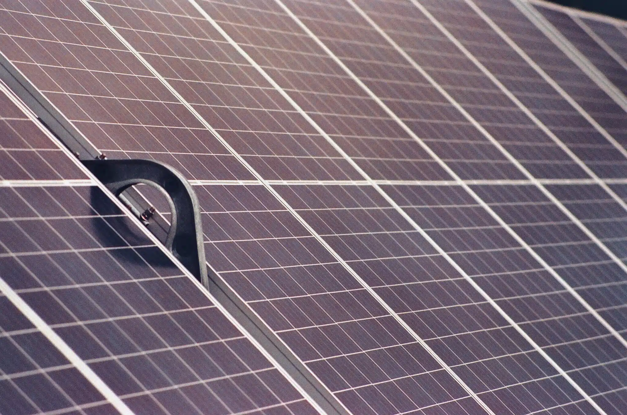
If you’ve shopped solar, you know that the default solar panel looks like a rigid black rectangle. But there is an alternative that can be lighter, thinner, and better suited to certain specialized applications. Thin film solar panels are an alternative photovoltaic technology that emphasizes different things in their design.
This beginner’s guide aims to explain what thin films are, how they’re made in contrast to silicon, their tradeoffs in terms of weight versus efficiency, the materials involved, and where they’re typically deployed. To understand where thin-film fits in the broader solar market, it helps to compare it with conventional crystalline silicon panels. After reading, you’ll understand where thin-film panels make sense and where conventional silicon panels are usually the better fit.
What is a Thin Film Solar Panel?
Thin-film solar panels are photovoltaic modules distinguished primarily by how they are manufactured. Instead of the traditional approach of sawing wafers from a silicon ingot to form individual cells, thin film panels are created by depositing extremely thin layers of semiconductor materials onto a substrate like glass, metal, or flexible foil.
Depending on the product, this can result in modules that are lighter than conventional framed silicon panels, especially in flexible or ultralight designs. The semiconductor layers themselves are very thin, often only a few microns thick, compared with much thicker crystalline silicon wafers. Some thin-film modules can be manufactured on flexible substrates, making them useful for curved surfaces or roofs where weight is a major constraint.
How are Thin Film Panels Different from Traditional Solar Panels?
To explain thin film, we first need to reference the dominant technology crystalline silicon (c-Si).
- Thickness and Material: Traditional panels are made from relatively thick crystalline silicon wafers. Thin-film panels instead use very thin deposited semiconductor layers. Many thin-film absorber materials are much more absorptive than crystalline silicon, so they can use much thinner active layers.
- Efficiency and Area: Crystalline silicon panels are usually more efficient per square foot than thin-film panels, which is why they dominate space-constrained applications like residential rooftops. Thin-film often needs more surface area for the same output, but the size gap varies a lot by technology. Modern CdTe modules are much closer to silicon than older low-efficiency thin-film products were.
- Heat Performance: Some thin-film technologies, especially CdTe, can have favorable temperature coefficients and strong energy yield in hot climates. That can make them attractive in very warm environments, although the gap versus modern silicon products is not always dramatic.
How Are Thin Film Panels Manufactured?
The process to manufacture thin film panels is comparatively quick relative to normal silicon photovoltaic processes which often require multiple factories/departments. Some thin-film manufacturers use highly integrated production lines that can turn coated glass into finished modules in only a few hours.
- Prepping the Substrate: Manufacturing starts with a large substrate such as glass, metal, or flexible foil. Instead of making individual wafer cells first, the thin-film layers are deposited directly onto that larger surface.
- Deposition: The semiconductor and contact layers are deposited using controlled vacuum or vapor-phase processes, with the exact method varying by thin-film technology and manufacturer. In some production setups, these coatings rely on materials supplied by sputtering targets manufacturers, particularly where film uniformity and deposition consistency are critical.
- Interconnection by Laser Scribing: Rather than wiring together many separate wafer cells after assembly, many thin-film modules use laser scribing to form monolithically integrated series connections directly on the substrate.
- Lamination: The finished layers are then encapsulated and protected. Some flexible products may omit the heavy aluminum frame used on many conventional modules.
What Materials Are Used in Thin Film Panels?
While crystalline silicon dominates the solar market, thin-film photovoltaics include several material families, most notably cadmium telluride (CdTe), copper indium gallium selenide (CIGS), and amorphous silicon (a-Si).
The technique for producing a panel in each family depends on how these materials are precisely combined and deposited. The exact layer stack depends on the thin-film chemistry, and performance depends heavily on precise control of those deposited layers. For example, modern CdTe designs may use cadmium selenium tellurium (CdSeTe) layers to improve light absorption.
What Are the Most Common Thin Film Techs?
While many experimental thin film panels exist, there are three main commercial families:
- Cadmium Telluride (CdTe): CdTe is the most commercially established thin-film solar technology at large scale. It uses much thinner active layers than crystalline silicon, and modern commercial CdTe modules are now in the high-teens to around 19%+ efficiency range, depending on the product generation.
- Copper Indium Gallium Selenide (CIGS): CIGS is a thin-film technology known for high research-cell efficiencies and the ability to be produced on flexible substrates. Commercial product efficiencies vary widely by manufacturer and application.
- Amorphous Silicon (a-Si): This non-crystalline form of silicon generally has lower efficiency than crystalline silicon outdoors, but it can be useful in specialized low-light or indoor-power applications such as small electronics and sensors.
Where Are Thin Film Panels Used?
Thin-film panels are much less common than crystalline silicon on residential rooftops because silicon usually delivers more power per square foot. Instead, they’re used in specific commercial/industrial situations:
- Weight-Sensitive Roofs: Lightweight thin-film products can be useful on commercial roofs where structural loading is a major concern.
- Hot Climates and Certain Diffuse-Light Conditions: Some thin-film technologies, especially CdTe, are valued for strong energy yield in hot climates and good real-world performance under less-than-ideal conditions. Exact performance depends on the module and project design.
- Irregular Surfaces: Flexible thin-film products can be used on curved surfaces, RVs, boats, building-integrated PV, and other applications where rigid framed panels are not a good fit.
Pros and Cons of Thin Film Solar Panels
Before deciding on thin film, it’s helpful to enumerate the operational distinctions:
Pros
- Heat Performance: Some thin-film technologies, especially CdTe, have favorable temperature coefficients and can hold up well in very hot conditions, though the advantage versus modern silicon modules varies by product.
- Flexibility: Can be applied to curves and are extremely lightweight.
- Potential Low-Light Advantage: Some thin-film technologies can perform relatively well in diffuse light and other suboptimal conditions, though results depend on the specific module and site.
Cons
- More Area Needed: Thin-film usually needs more surface area per watt than top-tier crystalline silicon, although the gap depends heavily on the thin-film technology and product generation.
- Lower Efficiency: While improving, typical thin film efficiencies are 6-15% versus 20%+ for modern c-Si.
- Lower Efficiency Per Square Foot: Thin-film modules often have lower efficiency than leading crystalline silicon modules, though modern CdTe products are now in the high-teens to around 19%+ range..
Final Verdict
Thin-film solar panels are not simply better or worse than crystalline silicon panels; they are designed for different constraints and use cases.Where roof space is limited, crystalline silicon is usually the better choice because it delivers more power per square foot.
Thin-film can make sense where weight, flexibility, surface shape, or extreme heat matter more than maximizing output per square foot. They excel when you have abundant area combined with flexibility and heat tolerance.